Saturday, December 28, 2013

How to import a graphic onto the PCB Overlay

How to import a graphic onto the PCB overlay | Altium Link : 

Use copy and paste images and text from Windows applications into Altium Designer. 
  1. Place the desired image into a Microsoft Word document
  2. Highlight the image in Microsoft Word and copy it to the clipboard (Edit->Copy in the menu)
  3. Open a new PCB in Altium Designer (File>New>PCB)
  4. Paste the image from clipboard (Edit>Paste)"
The image can be re-sized when it is first placed in Altium.


or the image can be re-sized before placing in Altium

'via Blog this'

Tuesday, December 17, 2013

PCB Layer Stack AD14

AD14 PCB Layer Stack Management | DOCUMENTATION: Altium

'via Blog this'

AD13 to AD14 - Custom Toolbars

After upgrading from AD13 to AD14 my custom toolbar which I created in AD13 was missing.

To restore my custom toolbar in AD14,  I copied the following three files from AD13 : 

DXP.RAF
DXP.RCS
UserTools.TLT

AD13 Location:
"C:\Users\Your User Name \AppData\Roaming\Altium\AD {xxx . . .}"

AD14 Location:
"C:\Users\Your User Name \AppData\Roaming\Altium\Altium Designer {xxx . . .}"


Tip: Altium must be closed while you copy the files, because the files are over written when a session of Altium is closed.

Just to be safe create copies of the AD14 files before overwriting them.


Dead Copper on Internal Plane layers between high density pins. | LinkedIn

Dead Copper on Internal Plane layers between high density pins. | LinkedIn

"PLACE' menu select 'POLYGON POUR CUTOUT' then draw a shape that surrounds the dead copper and right click to end shape. The copper will be gone inside the shape you just created. Fast and easy." 

Source: Jeri Deneen,C.I.D.+ Sr. PCB Designer 

 'via Blog this'

Monday, December 16, 2013

Altium Bug Crunch #960

Altium Bug Crunch #960: Altium Live Log in Required

Smart Length and Length Matching in PCB Editor

Fix in Development ?

'via Blog this'

Wednesday, December 11, 2013

Plane Dumb Copper

Unlike Polygon pours, planes in Altium do not have a remove dead copper feature.

You can place line or fills on the planes to remove copper. 


However this is an error prone method for removing dead copper because it relies on you reviewing and finding the dead copper with your eyeballs.


Altium Designer Summer 09 - Legacy Libraries

Altium Designer Summer 09 Libraries

  'via Blog this'

Friday, November 8, 2013

Drill Table - Bugs

As shown below you can get different results for the Drill Table in Altium depending on which method you choose to display your drill tables

Shown below are Drill tables for the same design with different results.


The new drill table shows a 124 holes.


New Drill Table ( Menu > Place > Drill Table)


While the legacy (.legend) Drill tables has 118 holes for the same design.  I believe when Altium created the new drill table the legacy table was inadvertently broken.

If you have legacy (.legend) drill tables in your older designs and you re-spin the board you need to delete the legacy (.legend) table and replace it with the new Drill Table. 

If you leave the legacy (.legend) drill table in your design, the drill table may not be in agreement with the NC Drill file.  

I had a couple projects on hold recently because the fab drawing was not in agreement with the drill files. I explained to my fabricator that I was using Altium, that they should follow the NC Drill file and ignore the Altium Drill table.

Also it is common to have dimmed rows in the the legacy table on the fab drawing as shown below if symbols are used to display the drills. The fix is to use characters.

The legacy Drill Table (.legend)

Symbols


As shown below changing the same legacy drill table above to use characters fixed the dimmed rows. 

Also if you have a lot of drills in the legacy table symbols may be repeated for different size holes, which is why another reason why characters should be used instead of symbols.

The legacy Drill Table (.legend)

Letters


I filed a bug (#3422) which has zero votes at Altium Live. So I'm not expecting to see a fix for the legacy drill table.

When I re-spin a board I need to remember to delete the .legend table and place the new drill table. 

PCB Release Failed


Another problem has surfaced, when using the PCB Release Manager to Generate Outputs.

Output generation failed with .legend (legacy drill tables).

Solution !!!

Always replace the .legend (legacy Drill Tables) with the new Drill Table.

PCB > Place > Drill Table


Sunday, October 27, 2013

Fix Connections - Script

The 'Fix Connections' script is a modified version of 'Fix Overlaps' which was created by Petar Perisin and can be found at Altium Addons.

Download Script Link:

I will describe in this post how I used the 'Fix Connections'  script on a recent DDR3 design.

As demonstrated in DDR3 Routing Simplified - Part 2  to get accurate length data we need cleanly connected routes in our designs.

I recently reviewed a reference design and noted that 500+ bad connections were found in the design.

Click on images to view


Let's clarify what the difference is for good and bad connections.

This design passed all DRC checks for opens and shorts, so in terms of connectivity there are no bad connections in the design.

However several of the length matched routes had bad connections in the design.  

These less than perfect connections resulted in wrong lengths being reported in the PCB panel for Total Net Lengths and the From -To Lengths.

Enter stage left, this where the 'Fix Connections' script shines.

As shown above 'All Nets' were checked for bad connections, however I wanted to verify the matched length routes in the DDR3 part of the design.

Using the drop down menu in the script I selected the 'DDR' Net Class which included all nets in the DDR3 circuitry and then selected Ok to run the script.


Note in this design there are also other DDR Net Classes that can be selected to focus on a specific data lane or the address and control lines.

By selecting a Net Classes and running the script I was able to easily find and fix the routes in the DDR Net Class.

Because the script remembers the last selected Net Class, I was able to quickly check and fix nets in selected Net Class.

Tip:

To further speed up the process the script was assigned to a custom menu and a hot key.

Conclusion


With a hot key set run the 'Fix Connections' script you can quickly find and clean up routes.

A big thank you to Petar Perisin, his efforts made this script possible.

Friday, October 25, 2013

Live Drill Table

Altium introduced the Live Drill Table in AD13.

The live drill table is scale-able which is nice, but I really don't see the value of the feature which updates the drill table every time I drop another via in the board. 

My main rant is that my fab drawings looked better when I used the old .legacy table.

For example here is screen shot of the .legacy


Click on images for better viewing


Below is what the same board  looks like after placing the new live drill table.


Nasty big graphic symbols, so crowded together that you can't tell what is what.

Also in the live drill table the option to use letters vice symbols appears to have been deprecated.

Sorry about the ranting today. AD14 was just released and with every new release I get a little angry. This because I'm getting tired of new features being introduced when in my opinion the Altium design software team should be focused on fixing bugs, adding better error handling to minimize the crashes and error reports.

As pointed out by Petr the Drill symbols can be scaled in the Outjob configuration.


Thursday, October 17, 2013

Design Rules Reference

"This comprehensive reference provides detailed information on setting up design rules 
for a PCB design. It also covers addition of rule-based parameters to objects in the 
schematic and Design Rule Checking. Detailed information for each of the individual 
rule types and their associated constraints is also provided."

Source: Altium Design Rules Reference 

'via Blog this'

Wednesday, October 16, 2013

Measuring code performance in Delphi Scripts

First step in code optimization is to determine which procedures in our code need to be optimized.

A millisecond timer is needed to test for the elapsed time required to execute the code.

On a Windows Machine we can use 'GetTickCount'.  Below is a code snippet for Delphi.

procedure TForm1.ButtonClick(Sender: TObject);
var
  startTick  : DWord;
  delta      : DWord;
begin
  startTick := GetTickCount;

  DoSomething; // Your Code

  delta := GetTickCount - startTick;
  ShowMessage(IntToStr(delta) + 'ms');
end;


See what CapnBry has to say about GetTickCount:

'via Blog this'

Delphi Basics

Delphi Basics:

'via Blog this'

Interactive Routing - Glossing - English documentation - The Altium Wiki

Interactive Routing - Glossing - English documentation - The Altium Wiki:

'via Blog this'

Saturday, October 12, 2013

DDR3 Routing - Simplified Part 2

DDR3 Routing - Simplified Part 1 

Part two of this series covers net length measurements and methods to ensure your matched length routes are properly implemented in Altium.

We will also look at a script 'Fix Connections' which is a modification of 'Fix Overlaps' that Petar Perisin created. 

Before we dive into using the '
Fix Connections' script, we will look at the accuracy of net length measurements in Altium.


Altium Net Length Bugs - Fact or Fiction


Have you heard that Altium has net length bugs ?   

Or that the 'From-To' data in the PCB panel is not accurate ?

I have seen messages on forums and blogs that claim Altium has bugs when it comes to extracting accurate net length data from the PcbDoc.  

Altium Bug Crunch #960: Altium Live Log in Required

I created a test case to prove if these reported bugs were fact or fiction.

Starting with a simple schematic which has three test point pads connected to the same net named "DDR_D1".


Defined a simple 4 layer stack up and ported the schematic to the pcb.


To simplify the math involved to check the accuracy of measured and reported net lengths the grid was set to 100 mil. 


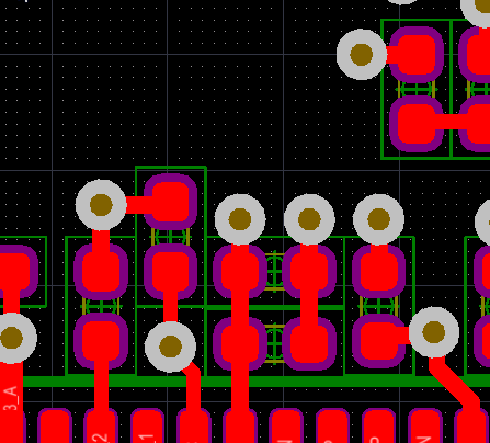
The design is displayed using the  2D transparent mode to allow for visual inspections of the routes.


With the Origin at the center of pad "A" as shown below.


As shown above I'm starting with all routes on the top layer.

Since the three pads  A,B,C are all on a 100 mil grid we know these lengths are:


A to the intersection = 400 mils

A to B is 400 + 300 = 700
A to C is 400 + 200 = 600
B to C 500

With origin set at the center of pad "A" it is a simple matter of double clicking on any of the three trace segments to bring up the properties dialog and verify the track lengths.


One popular way to get accurate track length data in Altium is to select one or more track segments and press "R" then "S" on the keyboard to display the length of the selected track segments. 


As shown below I have selected two of three segments and pressed the "R" then "S" key.


I am confident that Altium has reported this length correctly.

It would you be nice to be able to grab this measured data. Example press a command button to copy the measurement to your clipboard.

I submitted a feature request ( New Idea # 3279 ) to Altium, however it has not received much support.

Idea 3279

If you like this idea click on the above link and cast your vote.


Next we will use the PCB panel to examine the net lengths.


As shown above in the PCB panel the total length of the "DDR_D1" net is 900 mils, which is exactly correct.

Next we will examine the lengths between A,B,C using the From-To Editor


As shown above I selected in the second pane A-1 and B-1, then I added this selection to the 3rd (lower) pane.  As shown the A-1 to B-1 is 700 mils. Again I'm confident this is correct.

Now let's make things a little more interesting. 

I will drop a via at the intersection of A,B,C and move each of the three segments to different layers, then check the results.  Again I'm sure the results are correct.


Note that the measurements (AD13.3) do not take into account the via length as we transition from one layer to another.  

Regarding these layer transition lengths through the vias which are minimal.  It is up to you to determine if the via lengths are critical to the overall length of the nets in your project.  

Tip:

If you use the same number of vias and the same layers to route a data lane then the vias do not need to be accounted for.


Bad Connections


Next I will demonstrate how to get the reported bugs (bad length results).

I will change the grid from 100 to 1 mil and pull back the track on the top layer.


As show above I have pulled the track on the top layer a bit to the left so that is not centered in the pad at the 3-way intersection..

As show below we are now getting 688 vice 700 mil for the A to B path.


If I also pull the 'B' track the from the center of the intersection I can get a From-To length of 677 vice 700.  

Your net length results will vary depending on how many bad connections are in the net.

Let's look at what has happened to the total net length.  It is reporting 888 which is correct for total routed length of the tracks.


Note that the design will pass DRC checks for opens, because the tracks are contacting the pads.

Where are these reported bugs ? 

 "we have met the enemy and he is us"


Altium is reporting the actual routed track lengths.  

If you need accurate length data then route your tracks accordingly. 

Fix Connections Script 


Download Script Link:

Using this script we can quickly identify where the bad connections are and correct them.

With the tolerance set for 0.1 mil, select OK.


As shown below the script has found and highlighted the bad connection.


Conclusion:

Yes, Altium has problems reporting accurate trace lengths when the routes are not cleanly connected from point to point.  

Yes, Altium has issues when the routes have overlapping tracks, this includes tear drops.

Yes, Altium should create smarter net length measurement algorithms.

However:

If you don't apply teardrops, if you have no overlapping tracks, and you make clean connections you can get good results using Altium for High-speed designs.

Using the Transparent 2D view mode will allow you to see the bad connections.

The 'Fix Connections' script simplifies finding bad connections.


Thank you Petar ! ! ! 

DDR3 Routing - Simplified Part 1

Have you been led to believe that High Speed matched length routing in Altium is difficult ?

Routing DDR3 can be simplified in Altium provided you apply a few clever tricks and use a couple of scripts.

The scripts were created by Petar Perisin and can be downloaded at Altium Designer addons

Two of Petar's scripts are key to simplifying DDR3 routing.

Download Links:

Length Tuning Helper v1.0

Select Bad Connections v1.5


Length Tuning Helper 


Length Tuning Helper is simple to use and is an example of ingenuity.  This script solves the problem of creating matched length signals for designs which need to account for IC package pin delays.

The script can import Xilinx *.pkg or *.csv files.

I really appreciate the *.csv file option. 

The script also has an option for the units.

*.csv format example:

Units;mil
C3;563.55
B3;633.97
A2;558.13
A4;677.25
D3;567.52

In Excel the Pin Names and Pin Delay lengths are separated by a semi-colon in the same cell in column 'A' and the file is saved in the *.csv format.


Using the script is a simple four step process.  With *.PcbDoc selected in Altium run the script and . . .
  1. Select your DDR3 IC reference designator from a drop down menu. 
  2. Select Open File to browse and select the *.pkg or *.csv file.
  3. Select a Net Class from a drop down menu.
  4. Select OK


The script will add tracks above the design which are equal in length to the pkg pin delay data.

Here is an example of 32 data bits including DQSx and DMx signals


These track segments have been assigned the appropriate net names.

Now, the only thing left to do is to route the data lanes to the matched length requirements.

Once the routes have been matched you can delete these temporary track segments.


Thank you Petar ! ! ! 


Tip: Save these temporary tracks in a *.pcbdoc and add this *.pcbdoc to your project, then you can copy and paste these tracks back in to the design as needed. 

Use Edit > Paste Special to preserve the net names when copying the tracks.


In DDR3 Routing - Simplified Part 2 I will demonstrate why you should use Petar's 'Select Bad Connections' script.

Friday, September 20, 2013

Grid Settings - Easy on the Eyes

The default bright white grid lines and dots are a bit distracting and hard on the eyes. 

For a softer look that is easier on the eyes the color setting for the grid lines and dots can the adjusted.

Select Ctrl + G to bring up the Cartesian Grid Editor dialog.

As shown I have set the Dots to a med gray (color 34) and the Lines to a light shade of black (color 38).


Here is what the results look like.
Click on Image to View


Thursday, September 19, 2013

Toolbars - Move to Another PC

Refer to Link: Altium Forum Search:

C:\Users\username\AppData\Roaming\AD {<GUID>}

Where GUID is a long Set of Hex characters.

Use File Search if needed to locate the files shown below on your computer.

Copy the following files and paste it to the same location on your new PC.

DXP.RAF
DXP.RCS
UserTools.TLT 

Altium has to be closed, during this precedure, or else your copied files will be overwritten.

These files are overwritten when Altium is Closed.

If you are frequently updating your Toolbars, then Synctoy can be used to simplify this task.

 'via Blog this'

Update Schematic from Library

Altium BugCrunch #839 : 

 Position of refdes after update from library.
  1. Open SCH List Panel. Select All Objects > Include only Parts. 
  2. Copy current Orientation, and Mirror-status to a spreadsheet.
  3. Set to 0 and non-mirrored. 
  4. Perform library update.
  5. Copy spreadsheet data over SCH List data to recover original positions.
'via Blog this'

Friday, September 13, 2013

Excel - Conditional Formatting for Matched Net Lengths

Below is an example of using Green / Red (Go / No-Go) Conditional Formatting in Excel for checking matched trace length requirements.


Example