Tuesday, November 18, 2014

Developer | altium.com

Developer | altium.com:

Click on image to view


'via Blog this'

Defining & running Circuit Simulation analyses - English documentation - The Altium Wiki

Defining & running Circuit Simulation analyses - English documentation - The Altium Wiki:

How to define simulation models and its values on an ACCESS database - Altium Discussion Forums

'via Blog this'

Free PCB Design Tools | CircuitMaker


Why CircuitMaker

"You deserve something better. You’re part of the electronics maker and hobbyist community, and you’re coming up with amazingly cool and innovative things every day. We think you deserve better design tools, made specifically for you, to turn those great ideas into reality. That’s why we’re developing CircuitMaker.CircuitMaker will be a free PCB design tool powered by Altium. With a streamlined interface and powerful engine to boot, you’ll never have to worry about your software holding you back. This will be a free design tool unlike anything you’ve seen before."


Monday, November 3, 2014

PCB Libraries

PCB Libraries Expert - for Altium Designer

Click on image to view


PCB Libraries is my favorite tool for designing Altium footprints.

PCB Library Expert Overview - Video


"The new V2015 “PCB Library Expert” by PCB Libraries, Inc. has a new Altium Script Interface that imports both the Footprint and 3D STEP Model simultaneously and imports the Height and Description attributes straight from the FPX file. 


PCB Library Expert to Altium via Script - User Guide

Altium layer assignments are user definable. Also, the 3D Model rotates the same as the Footprint (if you rotate the footprint in Library Expert the 3D model will match the rotation). 


You can import one part or 10,000 parts at a time to create an entire new library using your personal library construction preferences."


Source: PCB Libraries - Tom Hausherr

I'll post a review covering the new features in V2015 soon . . .


Here are some great FP Designer videos (5 minutes each) –

Randy Clemmons CID+

Wednesday, October 22, 2014

Variant - Schematic

To create schematics for variants


In the out job Select 'Project Physical Documents'


In the Variant Manager menu Project > Variants

click on images to view


That's It.

Sunday, October 19, 2014

Polygon Pours - New Functionality


Key things to know when editing polygons in Altium 14.3 are:

1. Click and hold a handle for a moment before trying to move it.
2. Shift Space bar toggles the modes.

Source: http://bugcrunch.live.altium.com/#Bug/4421

Project Packager

The Project Packager can used to bundle up every file associated with a project and create a Zip file.

You can find the Project Packager under Project > Project Packager


Or Right Click on a Project and Select the Project Packager


click on image to view


Follow the defaults, select Next > Next > Next > Finish


Take a look in project's folder and you will find a zipped up copy of your project.


Tip: You can add other documents to a project that will be included in the Zip file.


I often add other files to a project such as BOM templates and stack up drawings.

That's It.

EEVblog #527 - Altium Entry Level PCB Tool Rant - YouTube

Gotta to love this guy

EEVblog #527 - Altium Entry Level PCB Tool Rant - YouTube:

'via Blog this'

Monday, October 6, 2014

PCB Libraries - Parts on Demand

PCB Parts on Demand - Part Data: 


I searched for ADA4940-2ACPZ-R7 at the Altium Content store and did not find the part.

I decided to try PCB Libraries - Parts on Demand and was pleasantly surprised to find the 
fpx file for this part was available.

I downloaded the ADA4940-2ACPZ-R7.fpx file and quickly created the footprint.

click on images to view


The tool has a user friendly graphical interface . 

Please mention my name when requesting your quote from PCB Libraries.

Thank you
Randy Clemmons CID+

Wednesday, September 3, 2014

PADS ASCII IMPORT BUG - PCBLIB ORIGIN OFFSET

Altium Bug Crunch
http://bugcrunch.live.altium.com/#Bug/4651

This bug was found in AD14.3.14  (latest release). 

Note AD14.2.5 Does not have this problem.

Most likely this bug was introduced into AD14.3.14 while making these enhancements.


Source: http://techdocs.altium.com/pages/viewpage.action?pageId=235578

Note the origin data error will be passed to the pick and place file data.

Steps to re-create the bug:

Download and Import this PADs ascii file INDC3225X280N.asc in to Altium using the import wizard.

Then make pcblib library. 

As shown below the pcblib file created from the pcbdoc has an origin offset.


Step by Step:

Import the PADs ASCII file at the link provided above.

click on images to view


After importing the PADS ASCII file, zoom to the center of the target (crosshairs) and note that the origin is correctly centered in the target.


Also a quick check of the pads properties shows the pads are properly centered about the origin. As shown below the left pad is located at X -1.47mm, Y 0mm


Also the right pad is correctly located at X 1.47mm, Y 0mm

So far everything is correct. 

Now let's create a pcblib from the imported PADs ASCII file (the Altium pcbdoc) and zoom in to view the origin in the PcbLib.

As shown below there is an offset error in the origin.


This is serious flaw for anyone who is importing PADs asc data and generating Altium library parts. 

This incorrect origin data will be passed to the pick and place file data. 

Also the origin error will adversely affect part placement base on the part's origin.

Checking the Left and Right Pad X & Y properties also shows there is and offset error.

Left pad X -1.4827mm,  Y -0.0127mm


and the right pad X 1.4573mm, Y -0.0127mm


Work-arounds:

  1. Manually move the origin in pcblib to center of the target (crosshairs).
  2. Select Edit > Set Reference > Center
Summary:

Be aware that when importing PADS ASCII data that until this bug is fixed you may need to move the origin in the pcblib files generated after using the import wizard and creating pcblib libraries.

If you have an interest in seeing this bug fixed, cast your vote at:
http://bugcrunch.live.altium.com/#Bug/4651


That's It

Wednesday, August 27, 2014

Polygon Cutouts - Altium Discussion Forums

Polygon is wrongly poured over polygon cutout - Altium Discussion Forums:

Workaround for Polygon Cutouts in AD14.3.14

"I tried this with a new, blank board.

I placed a polygon and then, a polygon cutout inside. The polygon cutout is not working. Then i have changed it to board cutout, and it works as expected. When i change it back to polygon cutout again, it works !!!


By the way, I found out, that it works, if you move the polygon."


Source: 

http://forum.live.altium.com/posts/204342/573029

'via Blog this'

Tuesday, August 26, 2014

Rooms - For Clearance Exceptions

Rooms are useful for creating exceptions. 

For example this Ethernet design called for 18 mils of clearance from the differential pairs to adjacent copper pours.

The diff pair nets were placed in class and a clearance rule was created to hold polygon pours back 18 mils.

click on images to view


This took care of the 18 mil (~3 x W) copper clearance requirement.


However as shown above, now there is a clearance error where the differential pairs connect to U500.

We can use a room to define a clearance exception for the differential pair at U500.

Define the Room

Design > Rooms


Tip: Use Shift + Click to Select an Existing Room

Tip: Select a handle on the Room > Drag Handle > Tab Key

Take note of the settings used for the room above, specifically:

Name RX_TX_ROOM

Not InComponent('U500') 

'Keep Objects Outside' 


Clearance Rule


That's It.

Monday, August 25, 2014

Drill Chart Properties


Selecting the new Drill Chart Properties can leave you frustrated.


Right Click the upper left handle in the table's corner to bring up the properties dialog.


Good luck, it's kinda of random that you will bring up drill table properties, more often than not you end up selecting a track in the table's frame.

Please let me know if you have a better method.

That's it.

Wednesday, August 13, 2014

Porting iMX6 Rex to AD14

iMX6 Rex is an open source reference board designed by FEDEVEL Academy.

The reference design was originally created using a AD13.  I'm between projects so I decided to port the iMX6 Rex design to AD14.3.13 and take a look at the design.

The iMX6 Rex module is an impressive credit card size reference design.  

You can learn a lot about high speed designs from Robert Feranec who offers to share his expertise through FEDEVEL Academy.

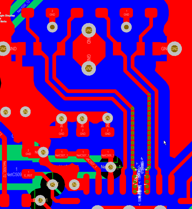
I loaded the Rex design in AD14.3.13 and ran the DRC checks for the PCB and found 3244 violations.

I also have AD13.3.4 (the last version of AD13) loaded on my PC, so I started this exercise with AD13 which reported 864 violations.


Loaded Rex in AD13.3.4


Clearance Constraint (Gap=0.085mm) ((IsRegion AND (OnLayer('L2') OR OnLayer('L11')))),(All)

These 864 clearance errors were most likely due to differences in 'Metric Display Precision' settings' on my PC and on the original designer's PC.

DXP > Preferences > PCB Editor > General


Re-pouring the polygons corrected the clearance errors in AD13. 

The design is DRC clean in AD13.


Rex in AD14.3.13

There were 3244 DRC errors reported in AD14.3.13.  These errors include the same 864 clearance errors reported in AD13.  

There were 2380 Differential Pair Width Rule violations due to the new Diff Pair design rules introduced in AD14.3 for differential pairs.


Diff Pairs Width Rules in AD13


After transferring the above Differential Pair width rules to AD14.3 only one DRC was reported for the Uncoupled length.


I suspect the Uncoupled length error is due the length calculation differences between AD13 and AD14.  

In AD14.3 the VIA lengths are included in the length data, which appear to have affected the Uncoupled length calculation.


After changing the Uncoupled length for the 'DIFF100' from 8mm to 8.7mm the design is DRC clean in AD14.3.13


Backward compatibility to AD13 

Note, there will be an extra set of width rules for the Diff Pairs which are not needed in AD14.3. 

If you do NOT delete the old Diff Pair width rules from AD13 then the AD14.3 design file with both old and new Diff Pair rules will be DRC clean in both AD13 and AD14.  

For backward compatibility leave the older AD13 Diff Pair width rules in the design.


Thank you Robert for sharing !

Tuesday, August 12, 2014

Output Job Page Setups


Schematic Prints (Color)


Assembly Prints (Gray scale)


Fabrication Drawings (Mono - Black)


For 11x17 PDF for page frames that are 11x17


Select Advanced


Select Source Document


That's it!