Creating a NPTH requires proper soldermask expansion and copper pullback from the edge of the hole. 3D Color View
If the design calls for a NPTH as show above (P2) a circle arc can be used to create the ring around the un-plated hole. Note that the soldermask was not pulled back from the edge of the hole for P1. The designer of this NPTH will get a technical query from the PCB fabricator asking for permission to pull back the soldermask from the edge of the hole. Shown in 2D the soldermask is correctly pulled back from the edge of the hole for P2.
Are we done Now ? . . . . . Before answering that question, let's look at typical surface mount pad.
Note soldermask expansion, which is typically 4 mils. The soldermask registration accuracy needs to be considered. More work is needed to properly finish this NPTH. Let's add a 5mil expansion to the arc (full circle)
Ok, now we are done. P2 is good to go.
There may be other factors to consider, like copper pours with same or different net than the ring around the hole.
Recently I reviewed a design where the Net names where not displayed in the Vias. I prefer to see the net names. To display the net names press "L" and select Show Via Nets in View Options. click on image to view
"ADIVA Announces Version 9.1 for Windows 7 thru 10.
Design validation has advanced another step with ADIVA's newest Release 9.1. This release includes a new interface to Altium Designer as well as enhanced support for Back Drill and Micro-Vias. " Source: ADIVA Corporation:
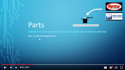
Parts is a free turn key working Access database for DBLib and SVNDBLib libraries. The Parts download includes an optional (not required) Frontend application that greatly simplifies creating parts and library maintenance. Parts can support 20 to 50 users. You can purchase keys for the Parts Frontend or create your own Frontend for the database. Get on the fast track with Parts.
If you are looking for a database with a web browser interface, take a look at ADLib. ADLib - Libraries Built to Last - Nine Dots Connect That's It !
Why use a region if you can use a room to define an area on the PCB? Answer: Rooms can only be used define an area on the Top or Bottom layers where the components are placed. While InRegion can be used to define an area on any layer of the design. Key points for using InRegion: 1) "All coordinates are referenced to the absolute origin (and not to the user origin or component insertion point), and at present, all coordinates always use units of mils. (1 mil = 0.001 inch)" Syntax: InRegion(X1 : Distance_String , Y1 : Distance_String , X2 : Distance_String , Y2 : Distance_String) : Boolean Tip: Use a temporary Fill to determine coordinates for X1,Y1,X1,X2
True Variants | Online Documentation for Altium Products: "There is also support for variations to component overlay information on the PCB, for example changing a components comment. This type of variation requires 2 overlay screens to be produced, resulting in 2, different bare boards. This type of variant is referred to as a Fabrication Variant."
How did I end up with duplicate unique IDs ? A new design was pulled together using sheets from prior designs. A couple of the sheets were duplicated in a new design using Save As to create some redundant circuitry. For example XVCR sheet was copied and saved as XCVR1 then again as XCVR2. Then both sheets were added to the project. Anyway, it was NO big deal and was easy to fix because the PCB had not been started.
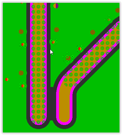
As shown below there is a bug in the tear drops, not all vias have tear drops.
Using Tools > Teardrops > Add > All > Vias
The work around: Shelve the polygons first, then create the teardrops, then re-pour the Polygons. Now the teardrops are properly generated.
Altium should alert the user to shelve the polygons before generating teardrops. Idea: create a smarter algorithm for generating the teardrops. Example ignore the teardrop / polygon violations while generating the teardrops, then fix the polygons during the next pour. That's it !
Vias violating clearance rule, where a No Net Keepout is being used. Using the rule below I'm able use the keepout, In the past I would replace the keepout with a polygon cutout. The end result is the same, however by using this rule I'm able to avoid creating the polygon cutout. click on images to view
Clearance Rule
OnLayer('L2 - GND PLANE') and IsKeepOut and IsVia Different Nets Min Clearance 3 mils (or what floats your boat).
In the PCB Panel you can Double Click on the xSignal Class to edit the Class. Click on image to View
The formula xSignals uses to calculate the via-used length is: StartLayerCopper/2+(Layers between StartLayerCopper and StopLayerCopper)+StopLayerCopper/2. That's it!
If you wish to display the same SVN Ver on all of your Schematic pages and *.PCBDoc.
*.SchDoc - Special String =VersionControl_RevNumber
*.Pcbdoc SpecialString .VersionControl_RevNumber
AD16.1.12 SVN# .VersionControl_RevNumber
In the Project Panel > Right Click on Source Documents > Open All. Then RClick Source Documents > Save All.
Then RClick on the Project.PrjPcb > Version Control > Commit Whole Project.
The .VersionControl_RevNumber works in the PcbDoc, however you may need to save, close and open the Pcbdoc to display the special stringl .VersionControl_RevNumber. You may need to first enter .VersionControl_RevNumber then edit the text string and add any prefixes or suffixes as desired, i.e. SVN# .VersionControl_RevNumber
The '.VersionControl_RevNumber' bug. Notice Altium will add leading and trailing single quote characters to .VersionControl_RevNumber string in the PCB editor, you must also remove the quotes.
In the schematic if the SVN Ver Number is not displayed, try holding down your Ctrl Key and roll the mouse wheel, the page should refresh and display the =.VersionControl_RevNumber string. One more PCB Special String Syntax example:
Anyone considering using a database library should take a look at what the guys at Nine Dots Connect have to say about libraries. Nine Dot Connects » Library Introduction & Philosophies Nine Dot Connects sells and supports ADLib from SolutionQuardant. ADLib runs in a Virtual Box and has a nice web browser interface. About Parts Parts is a turnkey Access database for Altium libraries which has been around since 2012. The Parts was designed to enhance Altium DBLib and SVNDBLib libraries. Parts supports multiple users on a company network drive (LAN). Parts has a desktop Frontend (GUI) that was designed by a professional librarian for the purpose of simplifying and expediting the creation of library components. Parts is also very popular with consultants and contractors because it can be installed on a laptop to create a portable library solution. See the 1 minute Video on YouTube


