Eric Albach
I just found a snippet design re-use method that is quite reasonable. Basically, append a question mark to the designators and create the snippets. Place the snippets in the new schamatic and PCB. Link the components between the schematic and PCB. Use Annotate Schematics Quietly. Update the PCB.
It's pretty easy. With this method it takes less than a minute to add a fully linked and annotated design. I used to spend a lot more time.
From the original schematic and PCB:
Update and Link the components between the schematic and PCB
Select the schematic section
Use SCH Inspector set to include only parts and use Smart Edit Formula on designators to append with a question mark.
Example formula : !+'?'
ends up with R12? (leaving the numbers keeps the components linkable and the question mark allows quiet annotation)
Update the PCB with the new designators
Create the schematic and PCB snippets
In the new schematic and PCB:
Place the snippets
Link the components using Project > Component Links > Add Pairs Matched by Designator
Use Annotate Schematics Quietly
Update the PCB
Source https://forum.live.altium.com/posts/221757/645999
Rich Betz
When you paste PCB snippets, be careful with existing 'ON' Planes. Your via's can and will connect to the first plane they contact, throwing your net connections all out of whack.
Either turn off all of your Plane Layers before you place the snippet, or place it outside the board outline until you get all of your component net connections linked up correctly.
When you get your Sch/Pcb component pin nets all linked up with All Layers On, select the whole snippet area.
Use PCB Filter (IsSelected and (IsVia or IsTrack)) to filter out the parts but hold on to all the connections.
Then CUT the connections with reference to Pin1 somewhere in the snippet,
Then Paste right back in the same place. All tracks and via's will adopt NetName from component pin nets.
Then... you can turn your Planes back on and position the snippet where you want it.
Source: https://forum.live.altium.com/posts/221757/646088
Eric Albach
Possibly the best method for the PCB side is to keep "snippets" in a PcbDoc then you can select, copy and paste special with Keep Net Name. That way you won't lose the polygon pour nets.
Source: https://forum.live.altium.com/posts/221757/646099
Tuesday, May 30, 2017
TrueType Fonts in PDFs
Workaround:
"Open the file in real adobe acrobat or the viewer rotate the pages and then rotate them back and then save. Files can now be saved. Doing this probably removes the bug that Thomas mentions and puts it back to the correct standard."
Source: Altium Ideas
"Open the file in real adobe acrobat or the viewer rotate the pages and then rotate them back and then save. Files can now be saved. Doing this probably removes the bug that Thomas mentions and puts it back to the correct standard."
Source: Altium Ideas
Sunday, May 28, 2017
Delphi File Basics
function Read_ini(junk:string):boolean;
var
folderName : string;
fileName : string;
myFile : TextFile;
data : string;
begin
//showmessage (Board.FileName);
//showmessage (PCBServer.GetCurrentPCBBoard.FileName);
//showmessage (ExtractFilePath(Application.ExeName));
//showmessage (ClientAPI_SpecialFolder_AltiumApplicationData);
// For ini file Saved in Project Folder
FileName := (ExtractFilePath(Board.FileName))+ 'Designators.ini';
// Global ini file
if Not FileExists(FileName) then
begin
// Try to open a text file for writing to
folderName := ExtractFilePath(ClientAPI_SpecialFolder_AltiumApplicationData) + 'Scripts\';
CreateDir (folderName);
FileName := folderName + 'Designators.ini';
end;
//showmessage (FileName);
if FileExists(fileName) then
begin
AssignFile(myFile, fileName);
// Reopen the file in read mode
Reset(myFile);
// Read the file contents
//while not Eof(myFile) do
//begin
//ShowMessage(data);
if not Eof(myFile) then ReadLn(myFile, data);
EditMinHeight.Text:= data;
if not Eof(myFile) then ReadLn(myFile, data);
EditMaxHeight.Text:= data;
if not Eof(myFile) then ReadLn(myFile, data);
EditCommentsTop.Text:= data;
if not Eof(myFile) then ReadLn(myFile, data);
EditCommentsBot.Text:= data;
if not Eof(myFile) then ReadLn(myFile, data);
EditTestPointsTop.Text:= data;
if not Eof(myFile) then ReadLn(myFile, data);
EditTestPointsBot.Text:= data;
//end;
CloseFile(myFile);
result := True
end;
// Debug Code
// Now see if the file exists
// if FileExists(fileName)
// then ShowMessage(fileName+' exists OK')
// else ShowMessage(fileName+' does not exist');
// Delete the file and look again
// DeleteFile(fileName);
// if FileExists(fileName)
// then ShowMessage(fileName+' still exists!')
// else ShowMessage(fileName+' no longer exists');
end;
function Write_ini(junk:string):boolean;
var
folderName : string;
fileName : string;
myFile : TextFile;
begin
// Open a text file for writing to
// For .ini files Saved in Project Folder
fileName := (ExtractFilePath(Board.FileName)) + 'Designators.ini';
AssignFile(myFile, fileName);
ReWrite(myFile);
Write(myFile, EditMinHeight.Text + #13#10);
Write(myFile, EditMaxHeight.Text + #13#10);
Write(myFile, EditCommentsTop.Text + #13#10);
Write(myFile, EditCommentsBot.Text + #13#10);
Write(myFile, EditTestPointsTop.Text + #13#10);
Write(myFile, EditTestPointsBot.Text + #13#10);
CloseFile(myFile);
// Global ini file
if Not FileExists(fileName) then
begin
folderName := ExtractFilePath(ClientAPI_SpecialFolder_AltiumApplicationData) + 'Scripts\';
CreateDir (folderName);
fileName := folderName + 'Designators.ini';
AssignFile(myFile, fileName);
//DeleteFile(fileName);
ReWrite(myFile);
Write(myFile, EditMinHeight.Text + #13#10);
Write(myFile, EditMaxHeight.Text + #13#10);
Write(myFile, EditCommentsTop.Text + #13#10);
Write(myFile, EditCommentsBot.Text + #13#10);
Write(myFile, EditTestPointsTop.Text + #13#10);
Write(myFile, EditTestPointsBot.Text + #13#10);
CloseFile(myFile);
end;
end;
Debug Code
// See if the file exists
// if FileExists(fileName)
// then ShowMessage(fileName+' exists OK')
// else ShowMessage(fileName+' does not exist');
// Delete the file and look again
// DeleteFile(fileName);
// if FileExists(fileName)
// then ShowMessage(fileName+' still exists!')
// else ShowMessage(fileName+' no longer exists');
Related Links:
Delphi Basics : Files
var
folderName : string;
fileName : string;
myFile : TextFile;
data : string;
begin
//showmessage (Board.FileName);
//showmessage (PCBServer.GetCurrentPCBBoard.FileName);
//showmessage (ExtractFilePath(Application.ExeName));
//showmessage (ClientAPI_SpecialFolder_AltiumApplicationData);
// For ini file Saved in Project Folder
FileName := (ExtractFilePath(Board.FileName))+ 'Designators.ini';
// Global ini file
if Not FileExists(FileName) then
begin
// Try to open a text file for writing to
folderName := ExtractFilePath(ClientAPI_SpecialFolder_AltiumApplicationData) + 'Scripts\';
CreateDir (folderName);
FileName := folderName + 'Designators.ini';
end;
//showmessage (FileName);
if FileExists(fileName) then
begin
AssignFile(myFile, fileName);
// Reopen the file in read mode
Reset(myFile);
// Read the file contents
//while not Eof(myFile) do
//begin
//ShowMessage(data);
if not Eof(myFile) then ReadLn(myFile, data);
EditMinHeight.Text:= data;
if not Eof(myFile) then ReadLn(myFile, data);
EditMaxHeight.Text:= data;
if not Eof(myFile) then ReadLn(myFile, data);
EditCommentsTop.Text:= data;
if not Eof(myFile) then ReadLn(myFile, data);
EditCommentsBot.Text:= data;
if not Eof(myFile) then ReadLn(myFile, data);
EditTestPointsTop.Text:= data;
if not Eof(myFile) then ReadLn(myFile, data);
EditTestPointsBot.Text:= data;
//end;
CloseFile(myFile);
result := True
end;
// Debug Code
// Now see if the file exists
// if FileExists(fileName)
// then ShowMessage(fileName+' exists OK')
// else ShowMessage(fileName+' does not exist');
// Delete the file and look again
// DeleteFile(fileName);
// if FileExists(fileName)
// then ShowMessage(fileName+' still exists!')
// else ShowMessage(fileName+' no longer exists');
end;
function Write_ini(junk:string):boolean;
var
folderName : string;
fileName : string;
myFile : TextFile;
begin
// Open a text file for writing to
// For .ini files Saved in Project Folder
fileName := (ExtractFilePath(Board.FileName)) + 'Designators.ini';
AssignFile(myFile, fileName);
ReWrite(myFile);
Write(myFile, EditMinHeight.Text + #13#10);
Write(myFile, EditMaxHeight.Text + #13#10);
Write(myFile, EditCommentsTop.Text + #13#10);
Write(myFile, EditCommentsBot.Text + #13#10);
Write(myFile, EditTestPointsTop.Text + #13#10);
Write(myFile, EditTestPointsBot.Text + #13#10);
CloseFile(myFile);
// Global ini file
if Not FileExists(fileName) then
begin
folderName := ExtractFilePath(ClientAPI_SpecialFolder_AltiumApplicationData) + 'Scripts\';
CreateDir (folderName);
fileName := folderName + 'Designators.ini';
AssignFile(myFile, fileName);
//DeleteFile(fileName);
ReWrite(myFile);
Write(myFile, EditMinHeight.Text + #13#10);
Write(myFile, EditMaxHeight.Text + #13#10);
Write(myFile, EditCommentsTop.Text + #13#10);
Write(myFile, EditCommentsBot.Text + #13#10);
Write(myFile, EditTestPointsTop.Text + #13#10);
Write(myFile, EditTestPointsBot.Text + #13#10);
CloseFile(myFile);
end;
end;
Debug Code
// See if the file exists
// if FileExists(fileName)
// then ShowMessage(fileName+' exists OK')
// else ShowMessage(fileName+' does not exist');
// Delete the file and look again
// DeleteFile(fileName);
// if FileExists(fileName)
// then ShowMessage(fileName+' still exists!')
// else ShowMessage(fileName+' no longer exists');
Related Links:
Delphi Basics : Files
Thursday, May 25, 2017
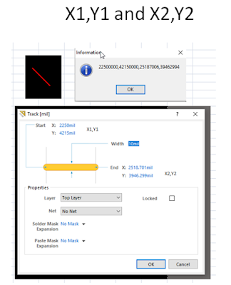
Track Coordinates X1,Y1 and X2,Y2
In Altium Track Coordinates are in mils x 10,000
click on image to view
click on image to view

Notes:
X1 is always less than X2.
Y1 can be less than or greater than Y2, it depends on the angle of the track and the starting location of the X axis.
That's it !
X1 is always less than X2.
Y1 can be less than or greater than Y2, it depends on the angle of the track and the starting location of the X axis.
That's it !
Monday, May 22, 2017
Find Dead Copper
Query to select all dead copper for deletion:
Modified Query - I added And NOT (Keepout = 'True')
(((((ObjectKind = 'Track') OR (ObjectKind = 'Arc')) And OnSignal)) Or IsVia) And NOT InAnyNet And Not InAnyComponent And NOT (Keepout = 'True')
Source Dennis Saputelli
https://forum.live.altium.com/#posts/221702/645693
That's it !
Modified Query - I added And NOT (Keepout = 'True')
(((((ObjectKind = 'Track') OR (ObjectKind = 'Arc')) And OnSignal)) Or IsVia) And NOT InAnyNet And Not InAnyComponent And NOT (Keepout = 'True')
Source Dennis Saputelli
https://forum.live.altium.com/#posts/221702/645693
That's it !
Friday, May 19, 2017
New in AD17.1.5
One of my projects has 3 Violations that did not exists in prior versions.

2 of 3 violations are related keep outs and the other violation is a soldermask web near via.
Lucky for me Altium included a new feature in AD17.1.5 that allows for selectively waiving DRC violations. Waiving DRCs is useful for backward compatibility.
Selectively Waiving DRC Violations | Online Documentation for Altium Products
New in AD17.1.5
Altium Designer 17.1 is now available (15 May 2017)
That's it !
AD17.1.5 Added support for object specific keepouts (BC:1424, BC:3483).
Legacy Workaround:
Tracks on other layers can be copied to the Global Keepout layer using Paste Special.
See: https://forum.live.altium.com/#posts/235870/716595
The New Way:
Added support for object specific keepouts (BC:1424, BC:3483).
Related links:
Altium Designer 17.1 is now available (15 May 2017)
Object Specific Keepouts | Online Documentation for Altium Products
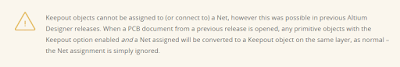
"In its simplest sense, a Keepout acts as an ‘interference’ object that prevents other copper objects from intersecting its area, as specified by the global Clearance Rule."
"Important Notice: The Keepout primitive cannot be added as a regular primitive now! Only the following menu command can be used for adding the Keepout: Place > Keepout. The target layer, where this limitation applies, can be set after the placement of the keepout. Starting with this release, there is no Keepout option in the properties of regular primitives, and vice versa, there is no ability to select a net, a mask or a solder paste in Keepout properties.
Altium forum: Keep-out layer unaccessable
My Comments:
Polygon pours will use global clearances rules to define the copper gap (pull back) and since the nets can not be assigned in AD17.1.5 to keep outs you will need to devise some new and cleaver ways to control the copper gaps in your RF designs.
I'm looking forward to using the new keep out features. However I need to beware that my older version designs are not backward compatible with AD17.1.5. Clearances rules that were associated with keep outs that had net names will need to fixed.
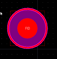
In AD17.1.5 my Fiducials now Fail DRC Checks.
My Fiducials, which where good for the past 7 years, are now NO Bueno.

Looks like it's time to re-design my Fiducials or Waive DRCs !
I chose to re-design my Fiducials :)
Keep outs and adjacent primitives (like Pads) must meet the global clearance requirements.
To fix my Fiducials I had to reduce the width of the arc and increase the radius.
That's it !
Tracks on other layers can be copied to the Global Keepout layer using Paste Special.
See: https://forum.live.altium.com/#posts/235870/716595
The New Way:
Added support for object specific keepouts (BC:1424, BC:3483).
Related links:
Altium Designer 17.1 is now available (15 May 2017)
Object Specific Keepouts | Online Documentation for Altium Products

"In its simplest sense, a Keepout acts as an ‘interference’ object that prevents other copper objects from intersecting its area, as specified by the global Clearance Rule."
"Important Notice: The Keepout primitive cannot be added as a regular primitive now! Only the following menu command can be used for adding the Keepout: Place > Keepout. The target layer, where this limitation applies, can be set after the placement of the keepout. Starting with this release, there is no Keepout option in the properties of regular primitives, and vice versa, there is no ability to select a net, a mask or a solder paste in Keepout properties.
Backward Compatibility: "All objects with the Keepout option turned on will be converted to Keepout primitives when the board is opened with this version of Altium Designer."
Altium forum: Keep-out layer unaccessable
My Comments:
Polygon pours will use global clearances rules to define the copper gap (pull back) and since the nets can not be assigned in AD17.1.5 to keep outs you will need to devise some new and cleaver ways to control the copper gaps in your RF designs.
I'm looking forward to using the new keep out features. However I need to beware that my older version designs are not backward compatible with AD17.1.5. Clearances rules that were associated with keep outs that had net names will need to fixed.
In AD17.1.5 my Fiducials now Fail DRC Checks.
My Fiducials, which where good for the past 7 years, are now NO Bueno.


Looks like it's time to re-design my Fiducials or Waive DRCs !
I chose to re-design my Fiducials :)
Keep outs and adjacent primitives (like Pads) must meet the global clearance requirements.
To fix my Fiducials I had to reduce the width of the arc and increase the radius.

That's it !
Tuesday, May 9, 2017
Rotated Octagons in Polygons and Planes
Here's simple and brilliant idea to improve signal integrity in Altium. This idea will allow users to push vias closer together and still have some copper poured between the vias, that's free signal integrity.
This idea was submitted by Per Magnusson on the Altium Ideas forum, check it out.
https://bugcrunch.live.altium.
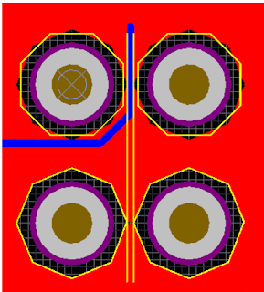
To create the eight sided Octagon in the polygon pours use a coarse Arc Approximation.
Example: Arc Approximation 5mil

If Altium will rotate the octagons shown above 22.5 degrees we will have larger copper webs between the vias under our BGAs which will improve signal integrity.
For hekkaidekagons 16 sided pullbacks the rotation should be 11.25 degrees.
The simple rotated eight sided octagons should improve polygon pour performance and they compliment 45/90 degree routing strategies.
Cast your vote at: https://bugcrunch.live.altium.
That's it !
Moving to Altium Designer from Cadence Allegro PCB Editor
Moving to Altium Designer from Cadence Allegro PCB Editor | Online Documentation for Altium Products:
When moving a design from Allegro to Altium, you may want to use the Allegro Viewer to verify the design was properly ported to Altium.
Using the Allegro Viewer is pretty straight forward, however here's a good tip.
To find stuff in Allegro . . .
Select the F4 key or Menu > Display > Element or select Show Element ( ! ) on the toolbar.
Then select the Find Tab . . .
 In the example shown above I'm searching for C314.
To Measure Stuff . . .
Select Display > Measure > Find > Shapes (only shapes) Pick two points.

That's it !
When moving a design from Allegro to Altium, you may want to use the Allegro Viewer to verify the design was properly ported to Altium.
Using the Allegro Viewer is pretty straight forward, however here's a good tip.
To find stuff in Allegro . . .
Select the F4 key or Menu > Display > Element or select Show Element ( ! ) on the toolbar.

Then select the Find Tab . . .

To Measure Stuff . . .
Select Display > Measure > Find > Shapes (only shapes) Pick two points.

That's it !
Sunday, May 7, 2017
My WorkFlow
Recently I was asked to share my workflow for designing printed circuit boards, so here it is . . .
About Me
I started my electronics career in the U.S Navy and worked with mil-spec requirements for 20+ years, then transitioned to commercial high-tech startups. I'm on my 4th high-tech startup, currently working at Ingenu.
You can find my resume and work history online at Linked In.
My Workflow
I release 20+ designs per year, my current duties includes company CAD Librarian, PCB Designer, Schematic Capture, BOM Generation, Fab and Assembly Drawings, which I upload to Agile (PLM) for review and release.
Here's an interesting series of PLM articles that I authored.
I use a Just in Time workflow, always keeping one step ahead my electrical design engineers. I mentor the team for all schematic capture related efforts and provide napkin drawings to schematic capture services if needed.
Up to 25% of the parts initially placed in schematics never make it to the layout stage, so creating footprints before the electrical design is frozen may be a waste of time. During the schematic design reviews I poll the team and determine which components are likely make it through the design reviews, then as needed I create footprints for those parts.
I use an Access database (Parts) which is lightening fast. Using drag and drop techniques I create similar parts in less than 15 seconds.
See Getting Started with Parts (YouTube 14 minutes) if you would like to see the Parts Frontend application in action.
I use PCB Libraries (Tom Hausherr's tool) to create footprints or download footprints from the Parts on Demand (POD) service. I was on the PCB Libraries beta team.
My favorite PCB calculator is the Saturn PCB Design Toolkit, created by Kenneth Wood. I collaborated with Ken to add and enhance features in the PCB Design Toolkit.
That's it !
Subscribe to:
Posts (Atom)