Thursday, December 19, 2019

Creepage and Clearance Rules

Please note Altium has made changes and improvements after the Creepage rule was introduced in AD20.

YouTube What is Creepage and Clearance ?   


PCB Creepage Calculator

In AD20 Altium introduced Creepage Rules

See AD20 Creepage Rule Bug


Queries with InLayerClass do NOT work :(


Note that Creepage and Clearance Rules are not the same thing.

Creepage is the length of path on the surface. Slots can be used to the path length.

Clearance the shortest distance between two points.

Slots and Creepage rules should not be used to satisfy Clearance requirements.

Example Clearance Rule


Note: InlayerClass('Outside') is only used in the Second Object Matches.

Related Links:


That's it !

Saturday, November 30, 2019

KiCAD ver 5.1.4 to Altium AD19.0.8

Assuming you have KiCAD source files.

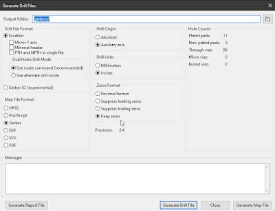
KiCAD > File > Fabrication Outputs > Drill


Precision 2,4

KiCAD > Plot Gerbers


Use Protel filename extensions.

Altium > New > CAM Doc (Camtastic)


File > Import > Drill. . .


Units. . .


Tool Table. . . 


Define Tool Table (Drill sizes)

Tables > Layers, set Top to Top and set Drill to Drill Int.
Tables > Layers Order > Set Physical Layers

File > Import > Gerber
Place > Flash
Tools > Netlist > Extract > Wait for it . . . 

File > Export to PCB

That's it !

Sunday, November 24, 2019

Importing xDxDesigner Schematics

xDxDesigner is  the schematic capture tool for Mentor Graphics Xpedition.

In altium the xDX Designer Importer extension (a Software Extension) can be found on the Purchased tab of the Extensions & Updates view (DXP » Extensions and Updates).

See: xDX Designer Importer | Online Documentation for Altium Products


Correct folder structure is important !


You may need to arrange the folders and files before importing xDxDesigner files.

See: Importing Dx Designer schematic to AD - Altium Discussion Forums

That's it !


Thursday, November 7, 2019

Rework Queries

(ObjectKind = 'Track') And OnSignal And (Net = 'No Net')

(ObjectKind = 'Track') and OnSignal and HasViolations


Find Dead Vias, Tracks and Arcs

(((((ObjectKind = 'Track') OR (ObjectKind = 'Arc')) And OnSignal)) Or IsVia) And NOT InAnyNet And Not InAnyComponent And NOT (Keepout = 'True')


Monday, November 4, 2019

Get Size From Sheet Layer

To Set the Sheet Size in the PCB Editor.

Assign a Mechanical Layer Type to Sheet


Select the Mechanical Layer > Properties > Other > Get Size From Sheet Layer


Tip: You can set the Layer Type back to N/A after using Get Size From Sheet Layer

That's it !

Sunday, October 20, 2019

Rats Nest Disappears when Dragging Components

If you are working with a large pin count BGA you may want to increase the PCB.ComponentDrag.ConnectionLimit.

Prefs > General > Advanced > PCB.ComponentDrag.ConnectionLimit

It would be great if Altium could automatically adjust the Connection Limits to support large BGAs.

Altium introduced a new feature in AD19 to re-route moved components, which is causing the rats nest to disappear. You may want to uncheck that new Interactive Routing feature.

Prefs > PCB Editor > Interactive Routing > Component re-reroute.

That's it !

Friday, October 18, 2019

Tips and Gocha's for Using Git with Altium

See Alan's Tips and Gocha's for Using Git with Altium


Thank you for sharing Alan !

Wednesday, September 25, 2019

AD19.1.7 Delete Footprint Primitives in a PcbDoc

Issues have been reported for deleting primitives from footprints in a PcbDoc.

Solution:

If the footprint is part of a Union, break the footprint out of the union.

Unlock the footprint location and unlock the primitives.

Now you should be able to move or delete the primitives.

Try Ctrl+Delete

If you are moving a pad, you may need to delete all tracks connected to the pad.

That's it !


Tuesday, September 24, 2019

AD19.1.7 - Pushing Tracks and Differential Pairs

Some routing issues have been reported which are related to the new glossing algorithm.

Altium forum link: I'm not drinking the ad18/19 Koolaid

Solution: Use the Legacy Glossing

Preferences > System > General > Advanced button > Check "Legacy.PCB.InternalGloss" > Close > OK > Restart AD

Thank you Tim !

Diff Pair not starting from selected tracks. Diff Pair Gap Setting ?

That's it !

Thursday, August 22, 2019

Variants - Toggle Fitted / Not Fitted

How to add a custom button to Toggle Fitted / Not Fitted Parts

How to select Variants - Altium Forum

That's it !

Copper Cleanup 'No Nets'

Copper Rework Cleanup:

NOT IsBoardCutoutRegion AND NOT InAnyComponent and ((OnSignal AND (ObjectKind = 'IsPolygon') AND NOT InAnyNet) OR (OnSignal AND (ObjectKind = 'Track') AND NOT InAnyNet And (Keepout = 'False')) OR  (OnSignal AND (ObjectKind = 'Arc') AND NOT InAnyNet And (Keepout = 'False')) OR (IsVia AND NOT InAnyNet And (Keepout = 'False')) or (OnSignal AND (ObjectKind = 'Region') AND NOT InAnyNet And (Keepout = 'False')) AND NOT InAnyComponent AND NOT (IsCutoutRegion = 'True')) or (ObjectKind = 'Region') AND (Area='0 sq.inch')

DRCs:

(Istrack or isVia or isArc) and OnSignal And Not InAnyComponent And HasViolations

Un-Routed Net Constraint: Region (0) . . . Dead Copper
(ObjectKind = 'Region') AND (Area='0 sq.inch')

Copper Cutouts:
(ObjectKind = 'Region') And (IsCutoutRegion = 'True')

Routing Filters:

((Istrack or isVia or isArc) and OnSignal And (Net = 'No Net') And Not InAnyComponent)

((Istrack and OnSignal ) or isVia ) And (Net = 'No Net')


((IsArc and OnSignal ) or isVia ) And (Net = 'No Net')

Planes:
(ObjectKind = 'Split Plane') And (Net = 'No Net')


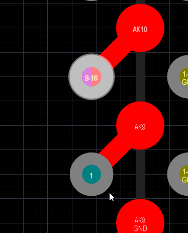
To keep an intentional Via Antenna convert the via to a free pad using Tools > Convert.


Select Long Routed GND Tracks
(ObjectKind = 'Track') And (Net = 'GND') and TraceLength > AsMils(50)

Select Short Routed GND Tracks
(ObjectKind = 'Track') And (Net = 'GND') and TraceLength < AsMils(50)


Select Long Routed PWR Class Tracks
(ObjectKind = 'Track') And (TraceLength > AsMils(50)) AND InNetClass('PWR')


Select Short Routed PWR Class Tracks
(ObjectKind = 'Track') And (TraceLength < AsMils(50)) AND InNetClass('PWR')


To Find small bits of tracks


(ASmm(SQRT((X2-X1)*(X2-X1)+(Y2-Y1)*(Y2-Y1))) < 0.2) and OnCopper

Optional  -  And NOT InAnyNet

That's it !


Friday, August 2, 2019

Export to AutoCAD

Typically Selected Options for Export to AutoCAD


That's It !

Wednesday, May 22, 2019

Pushing Tracks

Pushing tracks in Altium can be frustrating.

Try selecting the all of tracks you wish to push, hit the tab key to get all of track segments selected, then use Route  > Retrace Selected. 

Now try to push the tracks.

That's it !

Thursday, February 28, 2019

PCB Commands

Using Run Process in a script you can execute PCB commands.

I created a Delphi script which was running properly in both 2D and 3D modes with older versions of DXP (before AD18). After DXP migrated to 64bit the script would only run when the PCB was in the 2D view. I needed to add line of code to my script to switch from the 3D view to 2D.

Recently I learned to use RunProcess to execute PCB Commands in my scripts.

Example: To switch the PCB from 3D view to 2D view.

RunProcess ('PCB:Swithto2D')  / /  Delphi Script Code

RunProcess "PCB:Swithto2D"  ' VbScript Code

Link to Altium PCB Commands:
PCB Commands | Online Documentation for Altium Products

That's it !

Tuesday, February 26, 2019

Outjob - Copy Files

Example adding Fabricator's stackup to the project outputs using an Outjob.

Project Directory


Stackup files from Fabricator


Outjob > Copy Files


Configure Copy Files


Add and Edit
Output Container


That's it !


Friday, February 15, 2019

Working on the Grid

Component Grid

click on images to view


That's it !

Wednesday, February 13, 2019

Create Custom Toolbars

You can add custom Toolbars to Altium.

To add a Script to a custom toolbar, open the Script, then . . .

Right click on the main menu bar > Select Customize


Select Toolbars > New > Rename


Then select Commands > [Scripts] > Drag the Script to the custom menu.


Rename the menu button or add an icon if desired.

To add a button to a Custom Toolbar use drag as shown below.


That's it !

Monday, January 21, 2019

Hide the Active UI Toolbar


Select Preferences > System > General > Advanced 

Then uncheck UI.UseActiveBar

click on image to view


That's it !

Thursday, January 3, 2019

Joining Different GNDs

There are times when you need to short or join different nets together at a designated common point in a design such as AGND and DGND. 

In Altium this can be accomplished using NetTies if you have control of the schematic.

If you don't have control of the schematic you will not be able to include a NetTie symbol and NetTie footprint in the design.

One option is to create a short circuit in the design and waive the DRC violation.

For example you could join two different nets using overlapping fills or solid regions.

Another option if you don't want to waive DRCs is to create a rule that allows for the shorted nets.  

To prevent holds and technical queries from your PCB fabricator include notes in the fabrication package that include shorted nets.

That's it !

Flex-Rigid Design Links

Here is an Altium article titled "Best Practice of Flex Circuit Design"

https://www.altium.com/rigid-flex-circuits-resources/best-practice-flex-circuit-design


It's a bit dated, it was published when AD16 was released, however it is still relevant and has some of the best graphics I have seen related to flex designs.


Also see: 


Rigid-Flex Design - Altium Online Documentation

Coverlay Polygon - Altium Online Documentation
Bending Line - Altium Online Documentation

More flex resources:


Flexible Circuit Technologies is a highly regarded Flex resource.

Wurth Elektronik's also has some good stuff to share about designing with Flex-Rigid.

Video:

Advanced Rigid Flex Circuit Constructions - epec
Minimum Bend Radius Calculations


https://www.leiton.de/leiton-tools-flex-bendingradius.html

Best Technology - Asia


Tips:


Define Rigid-Flex Regions using View > Board Planning Mode


Select View > Board Planning Mode, then Select > Design > Define Split Line 

Snapping Options (Try Track Lines and a little cheese)


To delete a splitting line wiggle the line then press the delete key.

Enable All Objects in the Selection Filter to grab Splitting lines.


Show all Single Layers and Enable Regions to Define Stackup Regions


That's it !