Assuming you have KiCAD source files.
KiCAD > File > Fabrication Outputs > Drill
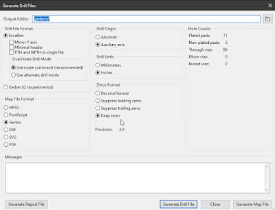 Precision 2,4
KiCAD > Plot Gerbers
Use Protel filename extensions.
Altium > New > CAM Doc (Camtastic)
File > Import > Drill. . .
Units. . .
Tool Table. . .
Define Tool Table (Drill sizes)
Tables > Layers, set Top to Top and set Drill to Drill Int.
Tables > Layers Order > Set Physical Layers
File > Import > Gerber
Place > Flash
Tools > Netlist > Extract > Wait for it . . .
File > Export to PCB
That's it !
(ObjectKind = 'Track') And OnSignal And (Net = 'No Net')
(ObjectKind = 'Track') and OnSignal and HasViolations
Find Dead Vias, Tracks and Arcs
(((((ObjectKind = 'Track') OR (ObjectKind = 'Arc')) And OnSignal)) Or IsVia) And NOT InAnyNet And Not InAnyComponent And NOT (Keepout = 'True')
To Set the Sheet Size in the PCB Editor.
Assign a Mechanical Layer Type to Sheet
Select the Mechanical Layer > Properties > Other > Get Size From Sheet Layer

Tip: You can set the Layer Type back to N/A after using Get Size From Sheet Layer
That's it !


