Altium Develop updates are supported in the Preferences

See https://forum.live.altium.com/#/posts/260310/845517
How to Change ProjectName in A365 Project Releaser
Regarding the area under the magnetics (transformer)
https://g.co/gemini/share/83c46504add6 - Gemini AI (Copper Keepout)
1GB Ethernet Length Matching Requirements - Gemini AI
That's it !
Select the Down Arrow to open the Advanced Properties
Source:
New pad dialog ain't so good - slots - Altium Discussion Forums
Via Stubs and Delay - GUI

The Script can find Via Stubs and Set Via Propagation Delay.
Enter the Max Stub length allowed in mils.
Select Top, Bottom or both to Find and Select Stubs.
Enter the desired max Via Stub length.
Double Clicking Max Stub will set Max Stub = to 1/2 Board's Copper Height.
For zero length stubs enter 0 in Max Stub.
Then select Run.
The script unshelves and repours polygons then starts checking the vias.
Store and Recall Buttons may be used to save and recall selected Via Stubs.
End or Via Stubs.
Via Propagation Delay Notes:
Select more or less than 1 Via to set the Propagation Delay of all Via Drill Pairs.Note Altium calculates the delay as the proportion of the via the signal path between the start and stop layers, this is not the physical ength of the via. It is the signal path electrical length.
Example: A board with a total thickness of 61.8mil, including a total of 1mil of solder mask and 2mil outer Cu thickness, where the electrical via length is calculated as Total - Soldermask - 1/2 top Cu - 1/2 bot Cu = 58.8mil.
Altium uses 1/2 of the copper height of the starting and stopping layers.
Example:
The Calculated Delay of the Via is 10.917pSec for a signal path length of 58.8mils.

Related Links:
https://resources.altium.com/p/your-complete-guide-stub-analysis
For more inforamation about this script Contact Parts (Randy Clemmons)
That's it !
To disable Auto Generate Supply Nets
Preferences > General > Advanced > Schematic.AutoGenerateSupplyNetsRule > Disable
Restart (Close and Open) Altium
See: https://forum.live.altium.com/#/posts/260254/848610
That's it !
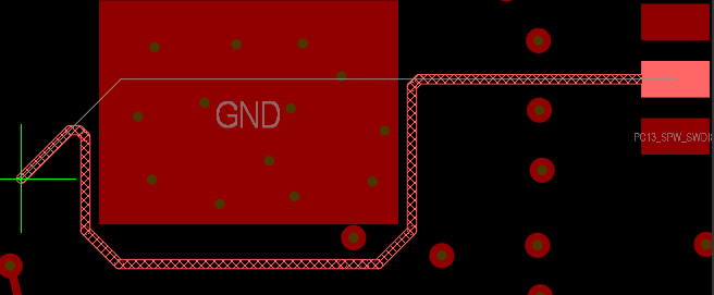
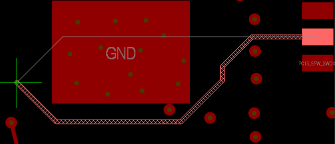
The Design Rule
Note:
Most designs should NOT include Not inAnyDifferentialPair in the Scope as shown.
This is a special case for the board used in this Return Path DRC feature review.
The example Rule shown above is targeting a specific Net Classes i.e. IS0. and S50
You may want to set the Scope to target All.
Gotcha 1
In Gotcha 1 the problem is the GND Via on the left has a signal routed between the flagged via and the GND Via.
Solution 1: Add another Via or Waive the Violation
Other Points of Interest:
Per online help
Exclude small areas of copper from flagging a violation by setting the required value (in sq. mils, 10 by default) of the PCB.Rules.ReturnPathIgnoreArea option in the Advanced Settings dialog.
That's it !
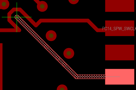
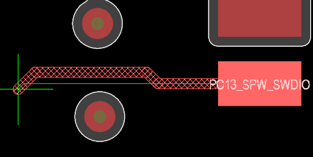
Ethernet PHY PCB Design Layout Checklist
The total length of each MDI trace should be less than 2 inches, or 2000 mils.
The traces should be lengthmatched within 20 mils for 1G transmissions and within 50 mils for 100M or 10M transmissions.
The number of vias and stubs on the MDI traces should be kept to a minimum.

The traces should be length- matched within . . .
20 mils for 1G transmissions
50 mils for 100M or 10M transmissions.
Also see Gemini AI: https://g.co/gemini/share/ee650e8e10c5
That's it !
See . . .
Using SDRAM vs. DDR RAM in Your PCB Design | Blog | Altium Designer
If you are looking for professional Altium Library design services and have a budget that can support the service then I highly recommend taking a look at . . .
Nine Dot Connects - Library Services
If you have a limited budget and like to do things yourself then I recommend you take Parts for free test drive.
Link to Parts https://pcbparts.blogspot.com/p/welcome.html
Parts is a Scalable Database Library Managment Solution for Altium users.
Parts can be used to quickly create and manage an Access or MySQL Database Library.
To request technical support or a Free Parts online demonstration contact me at Parts.
Link: Contact Parts
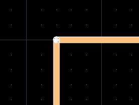
Interactive Routing Options - Online Altium (Login Required)
Gloss Effort (Routed) and Gloss Effort (Neighbor).
You may think of Gloss as a postprocessor: after the trace is put in and conflicts resolved, it straightens the result to get rid of corners and other uglies.
If it is Off, uglies are preserved, if Weak - the geometry of the trace mainly preserved, just locally smoothed, if Strong - the trace is made pretty much as short as possible.
See the pictures. Thin white line in all cases shows the trace as it was initially put in, then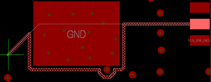

Design > Layer Stack Manager > Menu Back Drills


Customer's Requirements for 0.5mil Length matched Signals within the pairs.
Example
Sawtooth settings based on 6mil / 6mil (trace / gap) Diff Pair

Tip:
You have to select the type of tuning before you start tuning a net.
Hit Tab Key before you start the length matching
Thank you Wayne :)
Example six layer board with Corrupted Mid Layer IDs.
.Layer_ID and .Layer_Name
Example . . . Corrupt Mid Layer IDs
The Fix . . .
Backup the Project Design Files using Project > Project Packager
Open the PcbDoc . . .
Import Changes from Project to Update the Netlist and Design Rules in the PcbDoc.
Run DRC checks, take note of any reported errors.
Create and open a Copy of the PcbDoc in the project.
Design > Layer Stack Manager
Export Stackup as CSV, then include Impedance Screen Captures in Excel.
Delete all Mid Layers from the Corrupt Stackup.
Then add Mid Layers as needed.
Save Stackup to the PcbDoc, then check Mid Layer IDs and Layer Names.
Example Corrected Mid Layer IDs.
Design > Layer Stack Manager
Enter Material Thickness and Impedances as needed.
Save the fixed Stackup to the copy of the PcbDoc
Copy each Mid Layer from Original PcbDoc to Copy of PcbDoc.
Suggested Selection Filter Settings for Copying Mid Layers
Show all Mid Layers and use Signal Layer Mode.
Hide the Multi-Layer to avoid Selecting the Board and Board Cutouts.
Copy each Mid Layer from the Original PcbDoc to Copy of PcbDoc.
Use Edit > Paste Special > Check Paste on Current Layer and Keep Net Name.
Edit Design Rules and Fix Trace Width Rules as needed, including Diff Pairs.
Import Changes from Project to update the Netlist and Design Rules in the Copy.
Run DRC checks, take note of any reported errors.
Done !
Microsoft Word - Footprint Expert Surface Mount Families
Use the link above to download the 39 page PDF


That's it