In Sch editor, click command Tools » Convert » Reset Component Unique IDs
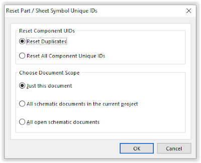 How did I end up with duplicate unique IDs ? A new design was pulled together using sheets from prior designs.
A couple of the sheets were duplicated in a new design using Save As to create some redundant circuitry.
For example XVCR sheet was copied and saved as XCVR1 then again as XCVR2. Then both sheets were added to the project.
Anyway, it was NO big deal and was easy to fix because the PCB had not been started.
That's it !
Here's a teaser. . .
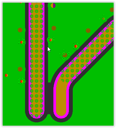
What's looks like a bunch of shorted nets?

Its a room !
This occurs when the Transparency setting is 0% for the rooms.
Fix: Change View Options > Transparency for Rooms to 60%
That's It !
As shown below there is a bug in the tear drops, not all vias have tear drops.
Using Tools > Teardrops > Add > All > Vias
The work around:
Shelve the polygons first, then create the teardrops, then re-pour the Polygons.
Now the teardrops are properly generated.
Altium should alert the user to shelve the polygons before generating teardrops.
Idea: create a smarter algorithm for generating the teardrops. Example ignore the teardrop / polygon violations while generating the teardrops, then fix the polygons during the next pour.
That's it !
Vias violating clearance rule, where a No Net Keepout is being used.
Using the rule below I'm able use the keepout, In the past I would replace the keepout with a polygon cutout.
The end result is the same, however by using this rule I'm able to avoid creating the polygon cutout.
click on images to view
Clearance Rule
OnLayer('L2 - GND PLANE') and IsKeepOut
and
IsVia
Different Nets
Min Clearance 3 mils (or what floats your boat).
That's It !
In the PCB Panel you can Double Click on the xSignal Class to edit the Class.
Click on image to View
The formula xSignals uses to calculate the via-used length is:
StartLayerCopper/2+(Layers between StartLayerCopper and StopLayerCopper)+StopLayerCopper/2.
That's it!