Interrogating Violations - English documentation - The Altium Wiki:
"There are essentially three methods of interrogating design violations - from the Messages panel, from the PCB panel and directly within the design workspace."
'via Blog this'
Thursday, August 29, 2013
DRCs - Interrogating Violations - English documentation - The Altium Wiki
Wednesday, August 28, 2013
Update PcbDoc From PcbLib
To update a PCB design from a PcbLib.
Open the *.PcbDoc and the *.PcbLib.
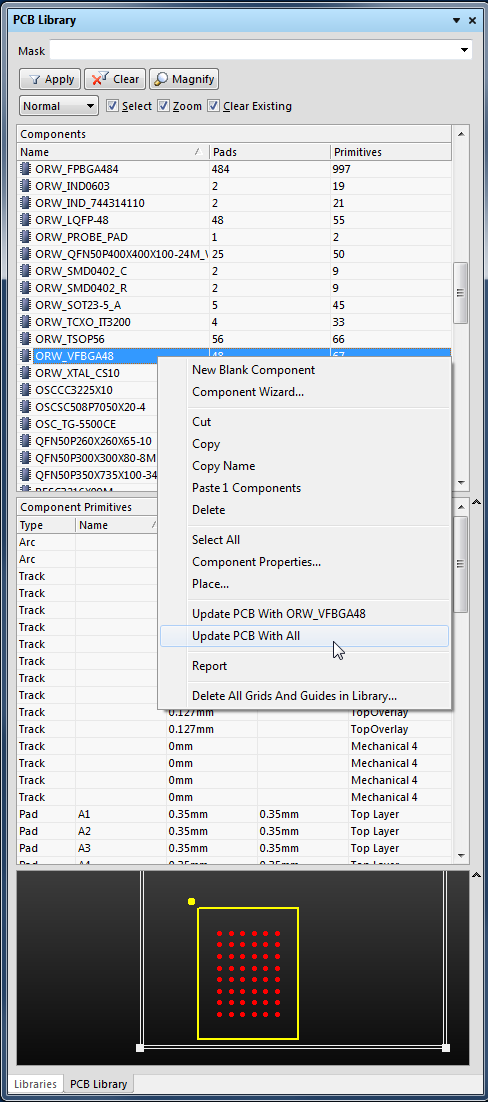
Select a Component in the PCB Library Pane, then Right Click to Update PCB with the selected component.
Or Update the entire PCB with all of the footprints with the same name parts by selecting 'Update PCB with All'.

Typical scenario, you need to update a PCB design and you may not have access to the libraries from which the parts originated.
First create PcbLib from the PcbDoc: Menu > Design > Make PCB Library
Modify the footprints as need then update the PcbDoc from the PcbLib following the steps described above.
Note that the PCB will be immediately updated without going through an ECO and a Report is not generated.
Open the *.PcbDoc and the *.PcbLib.
Select a Component in the PCB Library Pane, then Right Click to Update PCB with the selected component.
Or Update the entire PCB with all of the footprints with the same name parts by selecting 'Update PCB with All'.

Typical scenario, you need to update a PCB design and you may not have access to the libraries from which the parts originated.
First create PcbLib from the PcbDoc: Menu > Design > Make PCB Library
Modify the footprints as need then update the PcbDoc from the PcbLib following the steps described above.
Note that the PCB will be immediately updated without going through an ECO and a Report is not generated.
Wednesday, August 21, 2013
Routing - Auto Completion
Interactively Routing a Net - English documentation - The Altium Wiki:
"The Interactive Router is able to attempt automatic completion (Auto-Complete) of connections to the target pad, hold CTRL and Left Click to instruct the Interactive Router to attempt to complete the current connection.
This can make routing much faster than placing individual track segments, however, there are some limitations to Auto-Complete feature, as follows:
Start point and target pad are on the same layer The route can be completed in accordance with design rules (provided that routing conflicts are not being ignored).
Auto-Complete is available at any time, and you can even CTRL + Click directly on a pad or connection line to route it, there is no need to select it first.
You can use Auto-Complete on connections that are partially routed as well. To do this, CTRL + Click on the end of the last track segment or the remaining connection line to complete it to the target.
If a connection cannot be auto-completed the tool will return to the last used interactive routing mode."
'via Blog this'
Saturday, August 17, 2013
From-To Editor Features
Using the From -To Editor in the PCB panel will create dashed lines in your design.
The dashed lines look similar to the rats nest may cause you some concern.

To remove the dashed lines you will need to remove the From-To Pair in the PCB Panel.
Note: When the 'From To Editor' is selected the Rats Nest is not displayed.
The dashed lines look similar to the rats nest may cause you some concern.

To remove the dashed lines you will need to remove the From-To Pair in the PCB Panel.
Note: When the 'From To Editor' is selected the Rats Nest is not displayed.
PCBLib - Split Files Bloated
Embedded fonts create bloated files, single part PCBLib files that would typically only be ~65K will bloat to 488K in size.
True Type fonts may be embedded into each PCBLib file created when you run the Library Splitter Wizard.
The Embed True Type Fonts Option can be toggled in your Preferences.
DXP > Preferences > PCB Editor > True Type Fonts
Click to view
(Shown above Embed True Type Fonts Option is Enabled)
Steps to investigate and reproduce bloated file behavior:
Uncheck Embed True Type Fonts Option in your preferences.
Open a PcbDoc and Make PCB Library.
Design > Make PCB Library.
Note of the PcbLib File Size.
Check Embed True Type Fonts Option in your preferences.
Open a PcbDoc and Make PCB Library.
Design > Make PCB Library.
Note the PcbLib File Size is ~ 423K larger, due to the single instance of the embedded True Type Arial Font.
Split PCBLib
When a PCBLib is split with the Embed True Type Fonts Option Enabled, the True Type fonts are embedded into each of the split PCBLib files, creating bloated files.
To split a PCBLib:
Tools > Library Splitter Wizard.
Credits and References:
Ryan Rutledge uncovered this problem:
Reference Altium Live Bug 621: (Sign-In Required)
True Type fonts may be embedded into each PCBLib file created when you run the Library Splitter Wizard.
The Embed True Type Fonts Option can be toggled in your Preferences.
DXP > Preferences > PCB Editor > True Type Fonts
(Shown above Embed True Type Fonts Option is Enabled)
Steps to investigate and reproduce bloated file behavior:
Uncheck Embed True Type Fonts Option in your preferences.
Open a PcbDoc and Make PCB Library.
Design > Make PCB Library.
Note of the PcbLib File Size.
Check Embed True Type Fonts Option in your preferences.
Open a PcbDoc and Make PCB Library.
Design > Make PCB Library.
Note the PcbLib File Size is ~ 423K larger, due to the single instance of the embedded True Type Arial Font.
Split PCBLib
When a PCBLib is split with the Embed True Type Fonts Option Enabled, the True Type fonts are embedded into each of the split PCBLib files, creating bloated files.
To split a PCBLib:
Tools > Library Splitter Wizard.
Credits and References:
Ryan Rutledge uncovered this problem:
Reference Altium Live Bug 621: (Sign-In Required)
Labels:
DBLib,
Font Types,
Scalable True Type Fonts
Wednesday, August 14, 2013
SolidWorks Modeler for Altium Designer
"Moving files between different design systems is always a challenge. But why bother with import and export when both systems are running on the same machine?
With Desktop EDA’s SolidWorks Modeler for Altium Designer, take the next step into ECAD MCAD system integration.
This app for Altium Designer and its complementary add on for SolidWorks allows PCB designs to be edited in both systems without the need for an intermediate file"
Source Link:
'via Blog this'
Tuesday, August 13, 2013
Monday, August 12, 2013
DDR3 Design Guides
Design Guide for Two DDR3-1066 UDIMM Systems - Micron
Hardware and Layout Design Considerations for DDR3 SDRAM - Freescale
Video
DDR3 routing and PCB Layout - Robert Feranec
Sunday, August 11, 2013
Design Technology Notes - Smallest Features
Fab drawings often include design technology notes. The technology notes are used to identify the most advanced and challenging features within the design.
Typical Design Technology Notes include:
Minimum Trace Width.
Minimum Trace to Trace spacing.
Minimum Via Drill and Pad Size.
How would we find these minimum features in Altium ?
We can use a combination of 'Find Similar > 'PCB Filter' and 'PCB List' to find and identify the minimum size design features.
For example to find the smallest Via Pad size:
Start by selecting any small via in your design and use Find Similar.
click on image to to view
As shown above select 'Same' for Via Diameter. Note that the Create Expression and Run Inspector options are checked.
Shown at bottom of the PCB Inspector panel are the number of Vias found that matched the search criteria.
Nice, however recall what really want to know is what is the smallest Via pad size used in the design. Using Find Similar was a great way to get started and create a PCB Filter Expression with the proper syntax.
Next we modify the expression in the PCB Filter Panel to search for any Vias that are smaller. This is easily accomplished by changing the = 18 in the above example to < 18 and selecting apply.
(ObjectKind = 'Via') And (AsMils(ViaDiameter) < 18)
Looking again at the PCB Inspector Panel, we see there is a smaller Via size of 17mil used in this design. As shown at the bottom of the panel 44 objects are displayed.
Note if the Via Diameter size in the Inspector was displayed as <...> then there would be more than one Via size found with pad diameters of less than 18mil.
The steps shown above are useful to identify where in a design the smallest pad is used. In this example the smallest Via pad size of 17mil was used in 44 places to route a 0.75mm BGA.
We can also use the PCB Filter > PCB List (sorted) to find the smallest Via features for drill and pad sizes.
Using the same methods as described above you can identify the smallest line width.
For minimum Trace to Trace spacing refer to your design rules.
Wednesday, August 7, 2013
SiliconExpert | Electronic Components Database
Off Topic (Not Altium Related)
Sort'a like Altium Supplier Search Data, but on steroids.
SiliconExpert: "The leading data source for managing electronic parts SiliconExpert's parts database and tools keep your team up to date on over 250 million electronic parts. From obsolescence management to environmental regulation compliance and supply chain visibility, SiliconExpert empowers the electronics industry"
'via Blog this'
PCB Layout Transparency View
Using the Transparency View Option is a great way to critique how clean the routes are in a design.
The Transparency View Options settings are found under the View Configurations.
Design > Board Layers and Colors (Short key L)
You can quickly get into a transparent view mode by selecting the 'Altium Transparent 2D' View Configuration.
The Transparency View Options settings are found under the View Configurations.
Design > Board Layers and Colors (Short key L)
You can quickly get into a transparent view mode by selecting the 'Altium Transparent 2D' View Configuration.
Friday, August 2, 2013
3D Snap Points
For Circles, Cutouts, Holes
How do I get a snap point in the middle of a circle? - Altium WikiInteresting technique for cutouts, however it can be difficult to get the snap point precisely located at the center of the circle.
For Rectangles and Squares
To place a snap point at the midpoint of a rectangle or square two vertices need to be selected.
Example DE9 Connector Pins
Press the 3 key to switch to the 3D view.
Tools > 3D Body Placement > Add Snap Points from Vertices
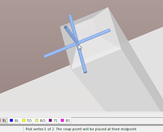
Follow the user prompts on the status bar at the bottom of the active window.
- Select Step Model Body
- Press Space Bar to enter the pick two vertices mode
- Select 1st Vertex
- Select 2nd Vertex
Select the 1st vertex

Select the 2nd vertex diagonal to the 1st vertex.
Result - Snap point is centered between the selected vertices.
Press Esc Key to Exit the Snap Point Placement mode.
Press the 2 key to return to the 2D view.
Press M > S for Move Selection.
Subscribe to:
Comments (Atom)


